
- 非IC关键词
企业档案
- 相关证件:

- 会员类型:普通会员
- 胡先生

- 电话:0755-85260989-2808/075585260989/075585260989
- 手机:18902444759//
- 地址:宝安区82区华丰科技园C座4楼
- 传真:0755-85260990-2822
- E-mail:forhu@xuyoe.com
产品分类
电源IC(10)二极管(5)三极管(6)场效应管MOSFET(18)光电子/光纤/激光(7)
- LED驱动IC(10)
- 桥堆/整流桥/桥式整流器(1)
- 快/超快/特快恢复二极管(1)
- MOSFET(17)
- 光电光耦合器(光耦)(2)
您的当前位置:深圳市世纪煦阳电子有限公司 > 元器件产品
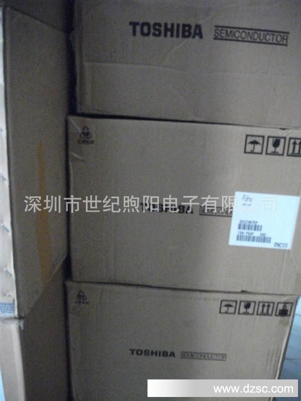

供应原装东芝2SK2837
品牌/商标:
TOSHIBA/东芝
型号/规格:
2SK2837
种类:
绝缘栅(MOSFET)
沟道类型:
N沟道
导电方式:
耗尽型
用途:
MOS-INM/独立组件
封装外形:
CER-DIP/陶瓷直插
材料:
N-FET硅N沟道
产品信息
品牌:东芝 型号:2SK2837 封装:TO3P
2SK3878
TOSHIBA Field Effect Transistor Silicon N-Channel MOS Type (π- MOSIV)
2SK3878
Switching Regulator Applications
• Low drain-source ON resistance: R
DS (ON)
= 1.0 Ω (typ.)
• High forward transfer admittance: ?Y
fs
? = 7.0 S (typ.)
• Low leakage current: I
DSS
= 100 μA (max) (V
DS
= 720 V)
• Enhancement model: V
th
= 2.0~4.0 V (V
DS
= 10 V, I
D
= 1 mA)
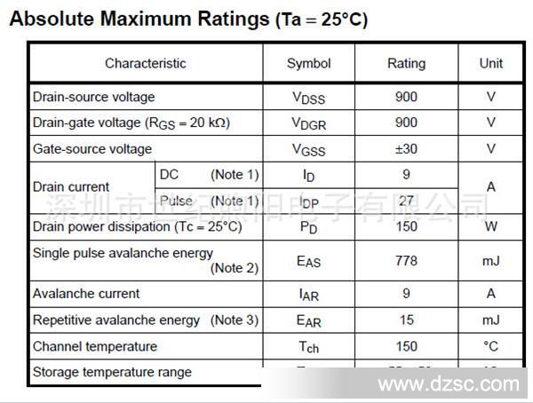
Absolute Maximum Ratings (Ta = 25°C)
Characteristic Symbol Rating Unit
Drain-source voltage V
DSS
900 V
Drain-gate voltage (R
GS
= 20 kΩ) V
DGR
900 V
Gate-source voltage V
GSS
±30 V
DC (Note 1) I
D
9
Drain current
Pulse (Note 1) I
DP
27
A
Drain power dissipation (Tc = 25°C) P
D
150 W
Single pulse avalanche energy
(Note 2)
E
AS
778 mJ
Avalanche current I
AR
9 A
Repetitive avalanche energy (Note 3) E
AR
15 mJ
Channel temperature T
ch
150 °C
Storage temperature range T
stg
−55~150 °C
Note: Using continuously under heavy loads (e.g. the application of high temperature/current/voltage and the significant change in
temperature, etc.) may cause this product to decrease in the reliability significantly even if the operating conditions (i.e.
operating temperature/current/voltage, etc.) are within the absolute maximum ratings. Please design the appropriate
reliability upon reviewing the Toshiba Semiconductor Reliability Handbook (“Handling Precautions”/Derating Concept and
Methods) and individual reliability data (i.e. reliability test report and estimated failure rate, etc).
Thermal Characteristics
Characteristic Symbol Max Unit
Thermal resistance, channel to case R
th (ch-c)
0.833 °C/W
Thermal resistance, channel to ambient R
th (ch-a)
50 °C/W
Note 1: Ensure that the channel temperature does not exceed 150°C
during use of the device.
Note 2: V
DD
= 90 V, T
ch
= 25°C, L = 17.6 mH, R
G
= 25 Ω, I
AR
= 9 A
Note 3: Repetitive rating: pulse width limited by max junction temperature
This transistor is an electrostatic-sensitive device. Handle with care.
TOSHIBA Field Effect Transistor Silicon N-Channel MOS Type (π- MOSIV)
2SK3878
Switching Regulator Applications
• Low drain-source ON resistance: R
DS (ON)
= 1.0 Ω (typ.)
• High forward transfer admittance: ?Y
fs
? = 7.0 S (typ.)
• Low leakage current: I
DSS
= 100 μA (max) (V
DS
= 720 V)
• Enhancement model: V
th
= 2.0~4.0 V (V
DS
= 10 V, I
D
= 1 mA)
Absolute Maximum Ratings (Ta = 25°C)
Characteristic Symbol Rating Unit
Drain-source voltage V
DSS
900 V
Drain-gate voltage (R
GS
= 20 kΩ) V
DGR
900 V
Gate-source voltage V
GSS
±30 V
DC (Note 1) I
D
9
Drain current
Pulse (Note 1) I
DP
27
A
Drain power dissipation (Tc = 25°C) P
D
150 W
Single pulse avalanche energy
(Note 2)
E
AS
778 mJ
Avalanche current I
AR
9 A
Repetitive avalanche energy (Note 3) E
AR
15 mJ
Channel temperature T
ch
150 °C
Storage temperature range T
stg
−55~150 °C
Note: Using continuously under heavy loads (e.g. the application of high temperature/current/voltage and the significant change in
temperature, etc.) may cause this product to decrease in the reliability significantly even if the operating conditions (i.e.
operating temperature/current/voltage, etc.) are within the absolute maximum ratings. Please design the appropriate
reliability upon reviewing the Toshiba Semiconductor Reliability Handbook (“Handling Precautions”/Derating Concept and
Methods) and individual reliability data (i.e. reliability test report and estimated failure rate, etc).
Thermal Characteristics
Characteristic Symbol Max Unit
Thermal resistance, channel to case R
th (ch-c)
0.833 °C/W
Thermal resistance, channel to ambient R
th (ch-a)
50 °C/W
Note 1: Ensure that the channel temperature does not exceed 150°C
during use of the device.
Note 2: V
DD
= 90 V, T
ch
= 25°C, L = 17.6 mH, R
G
= 25 Ω, I
AR
= 9 A
Note 3: Repetitive rating: pulse width limited by max junction temperature
This transistor is an electrostatic-sensitive device. Handle with care.